Stacked Microvias
Stacked microvias allow PCB designers to place vias in layers without adding an extra layer to the board. These vias look like pyramids from above and are drilled at different depths to create an interconnection between layers. They are especially useful when there is no room for larger vias or when there is a need to reduce capacitance between two sections of traces on a multilayer board. However, despite their advantages, stacked microvias pose some reliability issues.
When constructing a high-reliability microvia PCB, it is important to choose the proper materials. This includes both the underlying copper and the epoxy resin used to fill the holes. Poor choices can result in voids, which may lead to intermittent or complete failure. Voids can cause problems in the areas of the underlying copper and the solder connection. These can also cause issues with signal integrity, particularly in high-speed or power circuits.
The manufacturing process for a stacked microvias PCB involves drilling, plating, and filling with either pure copper or epoxy with copper. The plated copper is then soldered to the pads on the top and bottom surfaces of the board. This method of construction requires a more precise fabrication process than conventional PCBs. This is due to the small size of the microvia holes and the tight tolerances involved in the drilling. As a result, the holes must be carefully cleaned to ensure they are free of debris, residue, drill smear, fiberglass, and inorganic fillers before they are filled with copper.
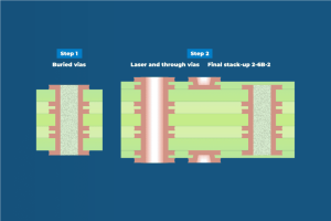
Materials Crucial for Stacked Microvias
Aside from their ability to improve PCB design, stacked microvias can be more cost-effective than traditional vias. This is because they require fewer processing steps to fabricate. In addition, they can reduce EMI radiation. This is because the stub lengths are reduced, which in turn minimizes signal reflection and interference.
Stacking microvias can also help increase the speed of a circuit. The smaller diameter of the microvias allows more current to flow through them, which improves signal quality. In addition, stacked microvias can reduce the number of plated through holes (PTH) needed on a circuit board. This allows for greater flexibility in routing and saves space.
To achieve a high-reliability microvia PCB, proper testing is crucial. This testing can include the following:
Several factors contribute to microvia reliability, including the thickness of the copper wrap plating and the copper bonding between the base of the microvia hole and the target pad. These factors can be improved through appropriate material selection, adherence to IPC-T-50M guidelines, and continuous resistance monitoring during the reflow process.
This will help to identify and correct any latent microvia failures before they cause a catastrophic failure. By following these practices, you can ensure that your stacked microvias are reliable and long-lasting. This will help to prevent a costly and time-consuming design redesign. To learn more about how stacked microvias can benefit your next PCB project, contact us today! We’re here to answer any questions you may have and help you find the best solution for your high-reliability application.