Microwave Circuit Board Enhance Design Flexibility
Microwave circuit board enhance design flexibility by addressing a variety of unique challenges. These include skin effect, coupling effect, impedance control and EMI/cross talk. These are a result of the high frequencies that RF/microwave PCBs support. To address these issues, designers leverage advanced simulation tools to optimize their designs before they go into physical realization. This enables iterative improvements that push the boundaries of high-frequency performance.
To achieve these performance metrics, microwave PCBs must have consistent gap and line width matching, precise copper weight and dielectric thickness, narrow slots in ground planes and buried vias, and angled edges that minimize internal reflections and discontinuities. Additionally, careful engineering of stub lengths, line widths and spacing, and the placement of passive components minimizes inductive and capacitive parasitics.
Moreover, the material selection for a microwave circuit board has a direct impact on its performance. The dielectric constant, loss tangent, and thermal properties of the chosen substrate determine the frequency response, impedance control, power dissipation, form factor, and reliability of the finished product. Engineers carefully evaluate these factors to select the best material for a given application.
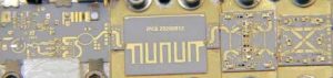
How Do Microwave Circuit Board Enhance Design Flexibility?
While many specialized construction techniques are used to achieve the performance and reliability needed for microwave applications, one of the most critical is the laminate. Microwave PCB laminates provide a foundation that supports the entire board. Specialized materials allow manufacturers to create a wide range of laminates that are tailored to specific applications. These materials also offer unique advantages that other PCB laminates cannot, such as lower Z-axis CTEs and a more stable chemical resistance.
In addition to the right material, the right PCB manufacturing process is also essential for achieving the performance required for microwave applications. This requires a highly-trained team of specialists who understand the unique needs of RF/microwave PCBs. This includes a thorough inspection protocol that assesses the quality of the dielectric materials and dimensional accuracy during production. In addition, accelerated life tests, environmental stress screening, and other quality assurance procedures are conducted to verify that the final products meet or exceed industry standards.
In addition to signal routing, microwave circuit boards often incorporate specialized components such as amplifiers, filters, mixers, and antennas, tailored to the specific requirements of the application. These components may be integrated directly onto the circuit board or connected via high-frequency connectors and interconnects, each requiring precise placement and routing to optimize performance.
Finally, microwave PCBs must be made with precision pads and plated connectors to avoid electrical failure caused by faulty connections. These failures can be caused by impedance discontinuities, reflections, and interference induced by minor fabrication defects that are not detected at lower frequencies. To ensure that these problems are not introduced during assembly, the manufacturer uses a combination of fine pitch soldering and wire bonding attachment methods, precise pad geometries, and plated through hole vias with angular edges to eliminate etch-back effects.