Buried Via Holes in Electronic Devices
Printed circuit boards (PCBs) use via holes to connect layers, facilitating the passage of electrical signals. While basic through-hole vias span the entire board, more advanced structures called blind and buried via holes connect between inner PCB layers without passing completely through the outer surface. These more complex via structures are particularly useful in high-density PCB designs. In this article, we’ll take a closer look at the underlying technologies, fabrication techniques, design considerations, reliability factors, and typical applications of buried via holes in electronic devices.
Unlike through-hole vias, a buried via hole is drilled from the inside of a PCB. This makes it more difficult to produce than through-hole vias, and it is often a significant factor in the overall price of a finished PCB. However, the advantages of buried vias make them an attractive option for many applications.
In addition to their manufacturing efficiencies, buried via hole also provide more space for components and routing by limiting the distance of signal paths. This helps to reduce parasitic capacitance and inductance, which improves signal integrity and overall device performance. Buried vias also allow for higher density in PCBs, as they can connect internal layers without affecting the surface layout.
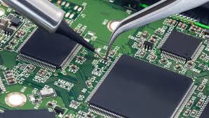
The Typical Application of Buried Via Holes in Electronic Devices
While buried vias have numerous benefits, they are not without their drawbacks. In some cases, using too many buried vias can create unintended issues like excessive signal interference and thermal stresses. To minimize these risks, designers should utilize advanced PCB design tools with built-in via management features. These tools can optimize via placement and suggest alternative routing strategies, minimizing the number of buried vias needed in the final product.
Another important consideration when using buried vias is their impact on the mechanical reliability of a PCB. Vias can concentrate thermal stress, which requires careful analysis and inspection for high-reliability applications. In addition, if a buried via fails, it can be very difficult to repair without removing the entire board from service.
A buried via hole is a type of via that connects internal layers of a PCB but does not extend to the outer surfaces. Unlike through-hole vias, which span the entire thickness of the board, or blind vias, which connect an external layer to an internal layer, buried vias remain completely enclosed within the PCB’s structure. This feature allows designers to utilize the board’s internal layers for interconnections without affecting the surface area, providing more room for components and traces on the outer layers.
The process of creating buried via holes involves advanced manufacturing techniques. During the PCB fabrication process, the internal layers containing the vias are laminated together before the addition of the outer layers. Laser drilling or mechanical drilling is typically used to form the via holes, which are then plated with copper to ensure a reliable electrical connection. This precise and controlled process demands high expertise and advanced equipment, making buried vias more expensive to produce than standard vias.
Despite these potential drawbacks, buried vias remain an essential tool in the PCB design process. By carefully planning the layer stack-up, utilizing automated tools, and collaborating with manufacturers, designers can ensure that buried vias are used in a way that maximizes their performance and cost efficiency.